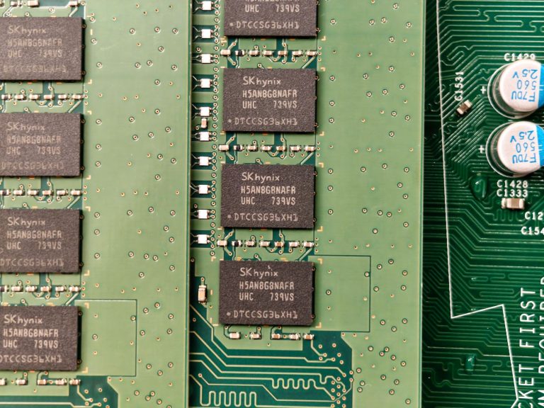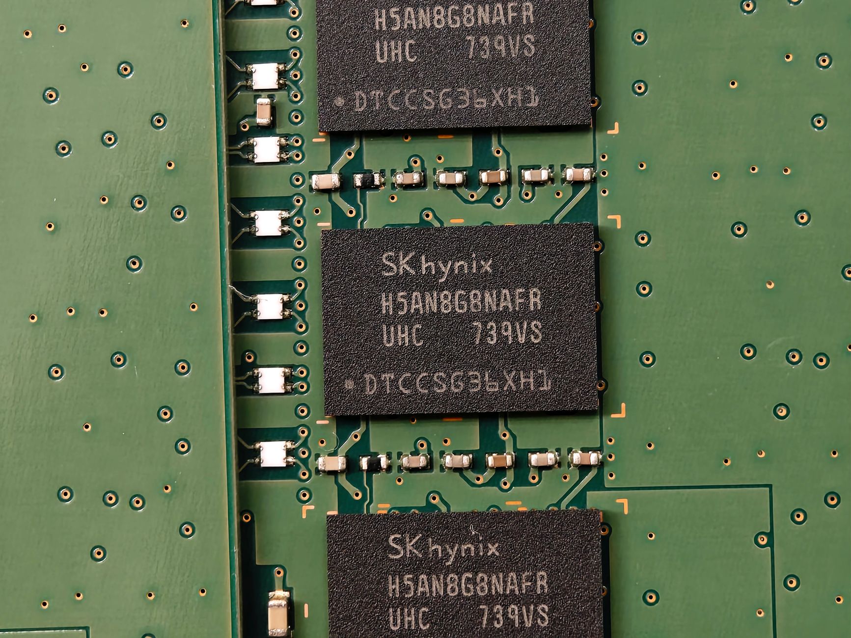
SK Hynix, the world’s second-largest memory chipmaker, will construct a new 20 trillion won ($51 billion) NAND flash memory fabrication plant (fab) in Cheongju, South Korea, with construction starting in 2025 and full-scale production targeted by 2029, according to a company announcement covered by ETTelecom. The new facility, dubbed “M17,” represents one of the largest single-site semiconductor investments globally and underscores a strategic bet by SK Hynix on sustained, long-term demand for high-density storage from artificial intelligence (AI) data centers, hyperscalers, and next-generation telecom network infrastructure. The announcement, made at an event attended by CEO Kwak Noh-jung and South Korean President Lee Jae Myung, highlights the critical role of advanced memory in powering the AI boom and the underlying data infrastructure.
Technical Deep Dive: M17’s Role in the AI-Driven NAND Evolution

The M17 fab is not merely an expansion of existing capacity; it is a foundational investment for the next generation of NAND technology. While SK Hynix has not released detailed technical specifications for M17’s output, the scale and timeline point to production of advanced 3D NAND layers beyond 500, potentially targeting 600+ layer stacks by the end of the decade. This aligns with the industry’s roadmap to increase bit density and reduce cost per bit, a critical metric for large-scale data storage.
For telecom network operators and infrastructure providers, the evolution of NAND has direct implications. The transition to 5G-Advanced and 6G networks, coupled with the virtualization of core network functions (vRAN, vEPC), demands storage with higher endurance, lower latency, and greater density. All-flash arrays in central offices and edge data centers are becoming standard for handling user plane functions and network slicing. Furthermore, the AI boom is not just about training models; it’s about inference at the edge. AI-powered network optimization, predictive maintenance, and customer experience management require high-performance, low-latency storage at aggregation points and cell sites, driving demand for enterprise-grade SSDs derived from leading-edge NAND like that planned for M17.
The $51 billion investment also covers the extreme ultraviolet (EUV) lithography equipment necessary for sub-10nm process nodes. This level of precision manufacturing is essential for producing the high-performance, power-efficient NAND chips required in modern servers and networking gear. The long lead time to 2029 production indicates SK Hynix is planning for technologies like Quad-Level Cell (QLC) and potentially Penta-Level Cell (PLC) NAND, which offer the highest densities for cost-sensitive, high-capacity applications prevalent in cloud and telecom backhaul storage.
Industry Impact: Supply Security, Pricing, and Competitive Dynamics
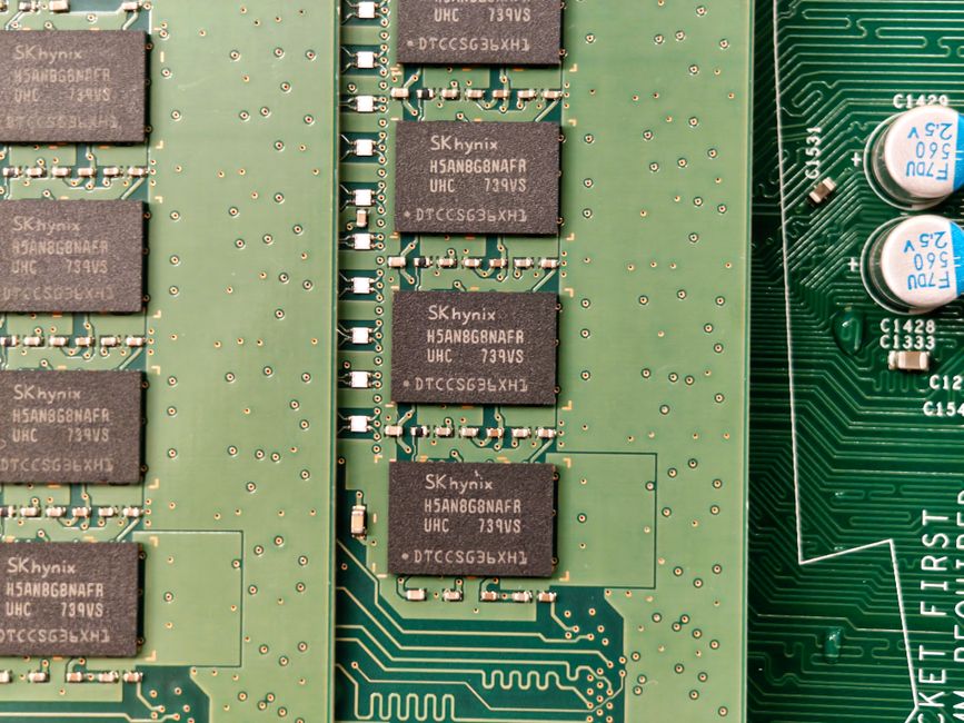
This massive capital expenditure (capex) signals a strategic shift in the memory industry, moving from a cyclical, demand-reactive model to one anticipating structural, long-term growth from AI and data infrastructure. For telecom operators and equipment manufacturers (OEMs), this has several key implications:
1. Supply Chain Security and Diversification: The concentration of advanced semiconductor manufacturing in South Korea and Taiwan has been a geopolitical concern. SK Hynix’s decision to build M17 domestically, with evident state support, reinforces South Korea’s “K-Semiconductor” strategy. For global telecom buyers, this adds a reliable, high-volume source of advanced NAND, potentially mitigating risks associated with supply chain disruptions. However, it also underscores the industry’s continued reliance on a few key geographies for cutting-edge chips.
2. Long-Term Pricing and Availability: While near-term memory markets are subject to fluctuations, a $51 billion commitment is a vote of confidence in sustained demand. This level of investment should help stabilize long-term NAND supply, preventing the severe shortages that can cripple hardware deployment schedules for network upgrades. For operators planning large-scale data center builds or nationwide fiber/5G rollouts requiring significant storage hardware, predictable component availability is as crucial as price.
3. Competitive Pressure on NAND Rivals: SK Hynix’s move pressures competitors Samsung and Kioxia/Western Digital to accelerate their own roadmaps and capex plans. This competitive intensity drives faster technological advancement, benefiting end-users through improved performance and cost metrics. In the telecom space, this translates to more capable and affordable solid-state storage for core routers, caching servers, and edge compute nodes.
4. Strategic Alignment with Hyperscalers: SK Hynix is a key supplier to cloud giants like Amazon Web Services, Google Cloud, and Microsoft Azure. These hyperscalers are also major investors in and consumers of global telecom infrastructure, from submarine cables to edge computing. The output from M17 will directly feed the storage needs of these companies’ global networks, which form the backbone of modern telecom services. A secure, advanced NAND supply chain is thus integral to the entire digital ecosystem.
Regional & Strategic Implications for Global Telecom Infrastructure
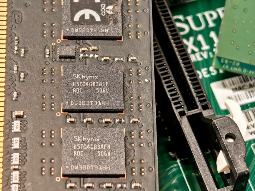
The location and scale of the M17 investment have broader implications for global telecom infrastructure strategy, particularly in high-growth regions.
Asia-Pacific Network Build-Out: The APAC region is the epicenter of both semiconductor manufacturing and explosive digital growth. Nations across Southeast Asia, India, and the Middle East are engaged in massive 5G deployments and national broadband network projects. The proximity of advanced NAND production in South Korea to these markets can streamline logistics and reduce lead times for critical network equipment. This supports faster rollout schedules and more responsive maintenance cycles for operators in these regions.
AI Readiness as a National Telecom Policy: South Korea’s support for the M17 fab is part of a national strategy to dominate the AI hardware stack. Other nations are making similar pushes. For telecom regulators and policymakers elsewhere, this underscores the need to consider the entire technology value chain—from raw silicon to network software—when crafting industrial and digital infrastructure policies. Ensuring access to advanced components like high-density NAND is becoming a matter of national competitiveness in the digital age.
Impact on African & MENA Telecom Markets: While geographically distant, African and MENA telecom operators are major consumers of the hardware enabled by chips like those from M17. As these regions leapfrog to 5G and invest heavily in data center capacity to meet local data sovereignty requirements, they depend on a stable global supply of advanced components. A significant, long-term investment in base-level memory technology helps de-risk their own infrastructure plans. Furthermore, as African operators explore AI for network optimization, fraud detection, and new services, the availability of cost-effective, high-performance storage will be a key enabler.
Forward-Looking Analysis: The Telecom Sector’s Silicon Dependency
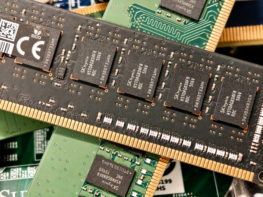
The SK Hynix M17 announcement is a stark reminder that the telecom industry’s future is inextricably linked to the fortunes and strategies of the semiconductor sector. The distinction between a “network” and a “data center” has blurred; modern telecom infrastructure is a distributed, software-defined data center. As such, its performance, efficiency, and cost are dictated by underlying silicon—not just CPUs, but also memory and storage.
Looking ahead, telecom operators must deepen their engagement with the semiconductor supply chain. This goes beyond procurement to include strategic partnerships, joint technology roadmapping (especially for edge and Open RAN hardware), and even potential co-investment in securing capacity for critical components. The era of treating memory as a commodity is ending; it is now a strategic differentiator for network capability.
Furthermore, the environmental, social, and governance (ESG) footprint of such a massive fab will be scrutinized. Telecom operators, under pressure to reduce their own carbon emissions, will need to factor in the embodied carbon of their network equipment. SK Hynix and other chipmakers will be pushed to power these fabs with renewable energy, a factor that may eventually influence procurement decisions of sustainability-focused operators.
In conclusion, the $51 billion M17 fab is more than a semiconductor factory; it is a cornerstone for the next decade of digital infrastructure. Its success will directly influence the cost, performance, and availability of the networks that will carry AI-driven services, immersive communications, and the global digital economy. For telecom leaders, understanding and planning for this silicon foundation is no longer optional—it is essential for future-proofing their networks.
About the Author