Huawei Unveils Tau Scaling, Shifts Telecom Chip Strategy from Transistor Density to Signal Speed
📰Original Source: ETTelecomIn a strategic pivot with profound implications for global telecommunications infrastructure, Huawei has unveiled a new chip design principle focused on signal speed rather than transistor miniaturization to circumvent U.S. sanctions limiting its access to advanced semiconductor manufacturing. According to a report by…
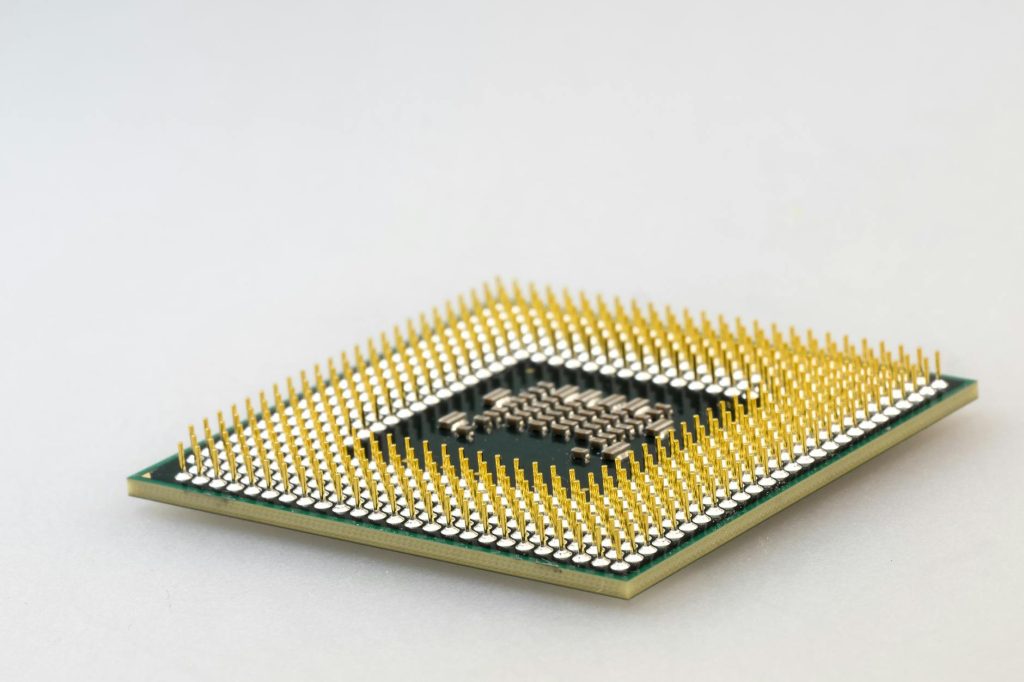
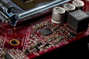
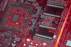
In a strategic pivot with profound implications for global telecommunications infrastructure, Huawei has unveiled a new chip design principle focused on signal speed rather than transistor miniaturization to circumvent U.S. sanctions limiting its access to advanced semiconductor manufacturing. According to a report by ETTelecom, the Chinese tech giant this week introduced the “Tau Scaling Law,” an alternative to Moore’s Law that prioritizes reducing signal propagation delay (tau, or τ) across chips and larger systems. This approach, which leverages architectural innovations like 3D stacking and its proprietary “LogicFolding” technology, aims to deliver performance gains for network equipment and smartphones without requiring access to the most cutting-edge sub-5nm fabrication nodes currently dominated by TSMC and Samsung.
Decoding the Tau Scaling Law and LogicFolding Architecture

The Tau (τ) Scaling Law represents a fundamental rethinking of performance optimization in computing and networking silicon. While Moore’s Law has driven progress for decades by shrinking transistor size to pack more onto a chip, Huawei argues that the focus must shift to minimizing the time it takes for electrical signals to travel across increasingly complex systems. This latency, measured in picoseconds, becomes a critical bottleneck in high-performance networking switches, routers, and baseband units where real-time processing is paramount.
Huawei’s implementation hinges on two key technical pillars. First is advanced heterogeneous 3D stacking, which vertically integrates different chip components (e.g., logic, cache, I/O) to drastically shorten the physical distance signals must travel between them. Second, and more novel, is the “LogicFolding” architecture. This design methodology, detailed in Huawei’s research, allows for the dynamic reconfiguration of on-chip logic gates and interconnects to create more efficient, shorter data pathways for specific computational tasks. In essence, it “folds” the logic to bring processing elements closer together on-demand, rather than relying on a fixed, less optimal layout. For telecom operators, this translates to potential gains in power efficiency and raw processing throughput for packet forwarding, signal encoding/decoding, and network function virtualization (NFV) workloads, even on chips manufactured at older, more accessible process nodes like 7nm or 14nm.
Impact on Telecom Equipment and the Global Vendor Landscape

Huawei’s chip strategy recalibration directly targets its core business: carrier-grade network infrastructure. By decoupling performance from the bleeding-edge foundry race, Huawei seeks to ensure the continued competitiveness of its 5G RAN (Radio Access Network), core network, and optical transport products. The company claims its Tau-optimized chips can deliver a 1.6x improvement in performance per watt for AI training tasks—a metric highly relevant for AI-driven network optimization and management. If validated in commercial hardware, this could allow Huawei to offer competitive or even superior power/performance specs in its base stations and routers compared to rivals like Ericsson and Nokia, who remain dependent on global semiconductor supply chains.
This development intensifies the bifurcation of the global telecom technology stack. Operators in markets friendly to Huawei, particularly across Asia, Africa, and parts of Latin America, may gain access to high-performance, cost-effective network equipment that is insulated from Western export controls. Conversely, operators in regions adhering to U.S. sanctions must continue to rely on the traditional Moore’s Law progression from a handful of chipmakers and OEMs. For infrastructure investors, this signals a deepening of two distinct technology ecosystems, with implications for interoperability, total cost of ownership, and long-term upgrade paths. The success of Tau Scaling could also pressure other equipment vendors to invest more heavily in architectural innovations and proprietary silicon design to maintain differentiation.
Strategic Implications for Emerging Markets and Network Sovereignty

The Tau Scaling initiative carries significant weight for telecom development in emerging economies, especially across Africa and the Middle East. These regions are priority markets for Huawei and are undergoing rapid digitalization with acute sensitivity to infrastructure costs. The ability to deploy advanced 5G and fiber networks using equipment that is both high-performance and potentially less expensive (due to relaxed manufacturing constraints) could accelerate rollout timelines. For nations pursuing “digital sovereignty” or looking to reduce reliance on Western technology, Huawei’s alternative R&D path offers a tangible option for building out national networks with a different supply chain backbone.
However, this path is not without risk. Operators must weigh the performance promises of Tau-optimized hardware against potential long-term challenges, including possible limitations in future scalability, vendor lock-in, and the evolving nature of international sanctions. Furthermore, the strategy’s success is predicated on Huawei’s ability to master complex chip packaging and integration—areas like 3D stacking and advanced interposers—which themselves require sophisticated and potentially sanctionable equipment. The durability of this architectural moat remains to be tested as competitors continue to advance both transistor scaling and their own packaging innovations.
Forward Look: A New Chapter in Telecom Hardware Innovation

Huawei’s public embrace of the Tau Scaling Law marks a pivotal moment, signaling that the era of homogeneous, process-node-driven progress in telecom silicon is over. The industry is entering a phase where heterogeneous integration, advanced packaging, and novel architectures like LogicFolding will be as critical as lithography for achieving gains in network capacity, latency, and energy efficiency. For network operators worldwide, the imperative is to deepen their technical evaluation criteria beyond mere teraflops or transistor counts, and to understand how underlying chip architectures impact real-world network performance, total energy consumption, and lifecycle costs.
The coming 12-18 months will be crucial for validation. As Huawei begins to integrate Tau-optimized chipsets into its flagship networking products, such as the Ascend AI processors and Kunpeng server CPUs, independent benchmarking by operators and industry consortia will reveal the true competitive impact. Regardless of the outcome, Huawei’s move has irrevocably shifted the conversation, compelling the entire telecom infrastructure sector to explore performance frontiers beyond traditional transistor scaling. This will fuel increased R&D in co-packaged optics, silicon photonics, and other technologies aimed at defeating latency, ultimately pushing the entire industry toward faster, more efficient, and more intelligent global networks.