
Imec CEO Calls for EU Chips Act 2.0 to Prioritize AI Chip Design for Telecom Sovereignty
📰Original Source: ETTelecomSource: ETTelecom, reporting on a statement by Imec CEO Patrick Vandenameele, “Imec CEO Urges EU to Strengthen AI Chip Design Initiatives in Upcoming Chips Act”, published May 20, 2026. The CEO of Imec, Europe’s premier nanoelectronics and digital technologies R&D hub, has issued…
Source: ETTelecom, reporting on a statement by Imec CEO Patrick Vandenameele, “Imec CEO Urges EU to Strengthen AI Chip Design Initiatives in Upcoming Chips Act”, published May 20, 2026.
The CEO of Imec, Europe’s premier nanoelectronics and digital technologies R&D hub, has issued a critical call for the European Union to sharpen its focus on AI chip design and collaborative frameworks within the forthcoming revision of its landmark semiconductor policy. Speaking ahead of the anticipated “Chips Act 2.0,” Patrick Vandenameele argued that while the EU’s initial €43 billion Chips Act correctly targeted advanced manufacturing and supply chain resilience, it must now pivot decisively to foster indigenous design capabilities for AI and high-performance computing (HPC) processors. For telecom network operators and infrastructure vendors, this strategic pivot is not merely about industrial policy; it directly impacts the future cost, performance, and sovereignty of the hardware underpinning next-generation 5G-Advanced, 6G, and AI-native networks. The EU’s ability to cultivate a competitive design ecosystem will determine whether European telcos remain dependent on foreign silicon for critical network functions like RAN acceleration, edge AI inference, and core network data processing.
The Design Gap: Why EU’s Current Semiconductor Strategy Falls Short for AI/Telecom

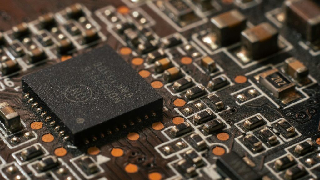
The EU Chips Act, formally adopted in 2023, was a geopolitical response to acute supply chain vulnerabilities exposed during the pandemic. Its primary objectives were to double the EU’s global market share in semiconductors to 20% by 2030 and mobilize over €43 billion in public and private investment, heavily weighted towards establishing state-of-the-art manufacturing fabs on European soil. Projects like Intel’s mega-fab investments in Germany and STMicroelectronics’ joint venture in France epitomized this manufacturing-first approach. However, Vandenameele’s critique centers on a structural imbalance: Europe possesses world-class research institutes like Imec (for process technology) and a handful of design champions (notably ARM, though UK-based, and NXP), but it lacks a robust, scaled ecosystem for designing the complex, power-efficient AI accelerators and HPC chips now demanded by the data-centric economy.
This design gap has profound implications for the telecom sector. Modern network infrastructure is increasingly defined by specialized silicon. Virtualized RAN (vRAN) workloads require hardware acceleration via DPUs (Data Processing Units) or SmartNICs. AI-driven network optimization and security rely on inference engines at the edge. The core network is evolving into a distributed AI compute fabric. Currently, European network equipment providers (NEPs) like Ericsson and Nokia, and telcos like Deutsche Telekom and Orange, source these critical components overwhelmingly from non-EU designers and foundries: NVIDIA (US) for AI training/inference GPUs, Marvell (US) for custom RAN accelerators, Broadcom (US) for switching ASICs, and TSMC (Taiwan) or Samsung (South Korea) for manufacturing. This creates a triple dependency: on foreign design IP, foreign fabrication, and geopolitical stability in Asia. Vandenameele’s call is to use Chips Act 2.0 to de-risk this dependency by making Europe a leader in designing, not just manufacturing, the chips that matter for future networks.
Impact on Telecom Operators and Network Infrastructure Vendors

A strengthened EU focus on AI chip design would have cascading effects across the telecom value chain, influencing vendor strategy, network total cost of ownership (TCO), and technological sovereignty.
For Network Equipment Providers (NEPs) like Ericsson and Nokia, a viable European design ecosystem offers a potential path to differentiation and supply chain control. Both companies already invest in custom silicon for baseband and radio units. Access to EU-supported advanced packaging labs, chiplet prototyping facilities, and design IP from research consortia could lower the barrier to developing more competitive, power-efficient ASICs for Open RAN and AI workloads. It could also facilitate partnerships with emerging European fabless design houses, reducing reliance on a handful of US-based merchant silicon vendors. The goal is not full vertical integration but securing a strategic multi-source option for critical components.
For Telecom Operators (OpCos), the implications revolve around cost, performance, and regulatory compliance. Indigenous European chip design could, in the medium term, exert downward pressure on hardware costs by increasing competition. More significantly, it could enable hardware that is architected for specific European needs: chips optimized for the energy efficiency mandates of the Green Deal, or with built-in security features aligned with EU cybersecurity certification schemes (e.g., EUCC). For operators building private 5G networks for industrial IoT, access to European-designed edge AI chips could be marketed as a sovereign, trustworthy solution for sensitive sectors like manufacturing, healthcare, and government.
However, the shift requires more than R&D funding. Vandenameele emphasized the need for “collaboration”—a reference to the fragmented nature of Europe’s tech landscape. Success hinges on creating viable platforms where NEPs, telcos, hyperscalers, automotive firms, and startups can co-design chip architectures. This aligns with initiatives like the European Processor Initiative (EPI) and KDT JU (Key Digital Technologies Joint Undertaking), but at a scale and speed matching US and Chinese efforts. Telecom operators, as major end-users, will need to actively shape these requirements through bodies like the GSMA or ETIS, ensuring the resulting silicon meets real-world network demands for latency, bandwidth, and programmability.
Global and Strategic Implications: A New Front in the Tech-Cold War

The Imec CEO’s intervention occurs within a high-stakes global contest for semiconductor supremacy, often termed a “tech cold war.” The US CHIPS and Science Act allocates billions, with strong incentives for leading-edge design and R&D. China is pursuing semiconductor self-sufficiency through massive state investment despite export controls. The EU’s initial Chips Act was seen as playing catch-up in manufacturing. Chips Act 2.0, by prioritizing design, represents a more nuanced and potentially more impactful strategy: aiming for leadership in specific, high-value segments like AI for edge computing, photonics-integrated electronics, and advanced packaging—all directly relevant to future telecom networks.
For the broader global telecom infrastructure market, a stronger EU design capability introduces a new variable. It could foster a “tri-polar” semiconductor landscape, reducing the current duopoly of US design/Asian fabrication. This diversification is generally positive for telecom buyers, enhancing supply chain resilience. It could also accelerate innovation in niche areas where European research excels, such as FD-SOI (Fully Depleted Silicon-On-Insulator) technology for low-power IoT and RF chips, or silicon photonics for co-packaged optics in data center switches—a technology critical for next-gen telco cloud infrastructure.
Regionally, this push has specific relevance for MENA and African telecom markets. These regions are themselves navigating digital sovereignty concerns and seeking partnerships for local infrastructure development. A sovereign European tech stack, from silicon to software, could present an alternative to solely relying on American or Chinese technology providers. Partnerships between European telco consortia and African operators could include technology transfer and training around Open RAN systems built on European-designed silicon, offering a differentiated path for network modernization.
Conclusion: The Road to Chips Act 2.0 and the Future of Network Hardware

Patrick Vandenameele’s call to action underscores a pivotal realization: semiconductor sovereignty in the age of AI is won at the design stage, not just the factory floor. The forthcoming Chips Act 2.0, expected to be debated in the European Parliament in late 2026 or 2027, will be a critical test of Europe’s strategic acuity. For the telecom industry, the stakes are clear. The hardware foundation for 6G (expected circa 2030) is being defined now through research into terahertz communications, integrated sensing and communication (ISAC), and native AI architectures. Without a seat at the chip design table, European telcos risk being perpetual technology takers, their network roadmaps and cost structures dictated by foreign silicon vendors.
The path forward requires a concerted, collaborative effort. It demands that telecom operators articulate their future silicon requirements with precision. It requires NEPs to deepen their chip design competencies and engage with European R&D pipelines. And it necessitates that EU policymakers channel funding not just into abstract research, but into practical platforms for chiplet innovation, design tool access for SMEs, and pilot production lines for telco-specific ASICs. If successful, the revised Chips Act could enable a new generation of “network-optimized silicon” born in Europe, strengthening the region’s position in the global telecom infrastructure race and providing its operators with a crucial lever for innovation and independence.