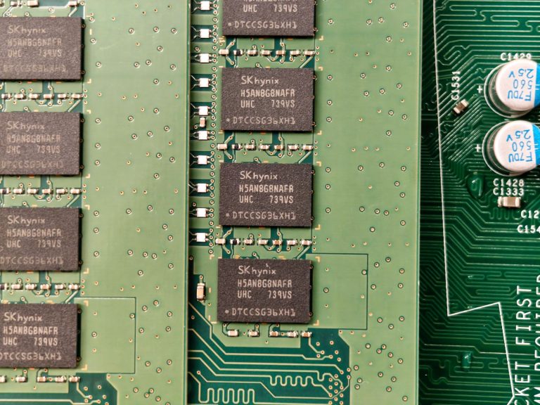
India’s strategic push to become a global semiconductor player is fundamentally a telecom infrastructure story, with design-led innovation emerging as the critical lever for achieving network sovereignty and reducing dependence on foreign hardware. According to an in-depth analysis by ETTelecom, industry leaders from NVIDIA, Intel, AMD, and Qualcomm, alongside government officials, are aligning on a vision where India’s $10 billion semiconductor incentive package must prioritize intellectual property (IP) creation and chip design to secure its digital future. For telecom operators and network infrastructure providers, this pivot is not about consumer electronics; it’s about controlling the silicon inside 5G/6G base stations, optical transport gear, core routers, and IoT modules. A robust domestic design ecosystem directly impacts supply chain resilience, network equipment costs, and the ability to tailor hardware for India’s unique scale and use cases, from dense urban deployments to affordable rural connectivity.
From Fab-Centric to Design-Led: The Technical & Economic Rationale

The global semiconductor value chain is bifurcated into design (high-value IP, R&D) and fabrication (capital-intensive manufacturing). For decades, India has cultivated a significant design talent pool, with over 20% of the world’s semiconductor design engineers reportedly based in the country, working for global giants. The new strategy, articulated by figures like Ashwath Rao, Director of Government Affairs at NVIDIA, argues for building on this foundation rather than attempting to leapfrog directly into cutting-edge fabrication (fab) nodes, which require upwards of $20 billion per facility and continuous multi-billion-dollar upgrades. A design-led approach focuses on creating proprietary IP for System-on-Chips (SoCs), networking processors, radio frequency (RF) components, and power management ICs tailored for telecom.
From a technical standpoint, this allows Indian entities to develop chips optimized for specific network functions. Imagine a 5G Open RAN Radio Unit (RU) chip designed for cost-effective, high-temperature operation in Indian climates, or a core network processor built with inherent security architectures mandated by local regulations. The economic model is also compelling. Design houses like ARM and NVIDIA operate with high-margin, asset-light business models, generating revenue through licensing and royalties. For India, this means capturing a larger share of the value from every piece of telecom equipment sold domestically and potentially exported. The government’s “Design-Linked Incentive (DLI)” scheme, part of the larger semiconductor mission, offers financial support and design infrastructure access to domestic companies, startups, and academia for developing chips, a move seen as essential to de-risk the initial R&D phase.
Industry Impact: Reshaping the Telecom Equipment & Hardware Supply Chain

The implications for telecom operators (MNOs), network equipment manufacturers (NEMs), and infrastructure investors are profound. Currently, the hardware stack—from Ericsson and Nokia’s 5G gear to Cisco and Juniper’s routers, and even fiber optic terminal equipment—relies on semiconductors sourced from a concentrated global supply chain (TSMC, Samsung, Intel fabs). A viable Indian design ecosystem introduces a new potential source for critical components, enhancing supply chain diversification post the COVID-era disruptions.
For Indian NEMs like Tejas Networks (now part of Tata Group) or Sterlite Technologies, access to locally-designed chips could reduce bill-of-materials costs, accelerate innovation cycles, and facilitate tighter integration between hardware and software, a key tenet of Open RAN and network virtualization. Pankaj Mohindroo, Chairman of the India Cellular and Electronics Association (ICEA), emphasizes that design is the “gateway” to manufacturing, suggesting that successful IP creation will naturally attract fab investments for volume production over time. In the interim, Indian-designed chips can be fabricated at foundries in Taiwan, South Korea, or eventually, within India’s own planned fabs like the Micron memory assembly plant or the proposed Tata-Powerchip fab.
Furthermore, global NEMs with large Indian R&D centers—such as Qualcomm (heavily invested in Hyderabad and Bengaluru for wireless tech) or Intel—may deepen their in-country design work, transitioning from back-office support to front-line IP development for global products. This elevates India’s role from a talent outsourcing hub to a strategic IP creation node within global telecom tech supply chains.
Strategic Implications for Network Sovereignty and the Global South

Beyond economics, the drive for semiconductor design capability is a core component of “network sovereignty”—the ability of a nation to control and secure its critical digital infrastructure. For India, with over 1.2 billion mobile connections and massive state-led projects like BharatNet, reliance on imported hardware poses strategic risks, including potential backdoors, export controls, and geopolitical leverage. Developing in-house design expertise for secure networking chips, encryption modules, and trusted hardware roots is a national security imperative alongside an economic one.
This strategy also positions India uniquely within the Global South and emerging markets. African and MENA telecom markets face similar challenges: price sensitivity, harsh environmental conditions, and a need for scalable solutions. India’s success in designing low-cost, ruggedized telecom silicon could create a new export category: “appropriate-tech” network hardware for emerging economies. Instead of merely being a market for Western or Chinese equipment, India could become a supplier of the core semiconductor IP that powers next-generation networks across Asia, Africa, and the Middle East. This aligns with India’s broader digital diplomacy efforts, such as the India Stack and its collaboration on digital public infrastructure.
The regional dynamic also includes countering China’s dominant position in both network equipment (Huawei, ZTE) and its aggressive $150 billion push for semiconductor self-sufficiency. While India is not aiming for direct head-to-head competition in advanced fabrication, a strong design ecosystem creates an alternative, non-Chinese source of innovation for the global telecom industry, which is increasingly wary of monolithic supply chains.
Forward-Looking Analysis: The Telecom Sector’s Silicon Future

The trajectory of India’s semiconductor ambitions will significantly influence the telecom sector’s capital expenditure (CAPEX) patterns and technological roadmap over the next decade. Success in design could lead to the first commercial deployments of “Designed in India” chips in field trial networks by the late 2020s, potentially targeting areas like 5G RedCap (Reduced Capability) for IoT, small cell baseband processors, or optical networking DSPs (Digital Signal Processors).
Operators should monitor this space for potential partnerships with domestic design startups, leveraging government sandboxes to test new hardware that promises lower total cost of ownership (TCO). Infrastructure investors must factor in the growing role of sovereign semiconductor policies in their risk assessments for network builds. The long-term vision is a vertically integrated stack where Indian software talent (already strong in network orchestration and automation) combines with Indian-designed hardware to create optimized, secure, and cost-effective network solutions.
However, challenges remain: retaining top design talent within domestic firms versus global giants, securing consistent venture funding for deep-tech semiconductor startups, and navigating the intense global competition for chip design tools (EDA) and advanced packaging technologies. The government’s role in creating a sustainable demand pipeline—through preferential procurement in public sector networks and BharatNet—will be as crucial as the financial incentives.
In conclusion, India’s design-led semiconductor strategy is a high-stakes gamble with direct ramifications for global telecom infrastructure. It moves the nation from being a passive consumer of network technology to an aspiring architect of its core components. For the global telecom industry, it signals the arrival of a new, talent-rich node in the innovation ecosystem, one that could reshape hardware economics and supply chain geopolitics for decades to come.
About the Author