Prime Minister Narendra Modi on July 5, 2026, inaugurated CG Power and Industrial Solutions’ (CG) Outsourced Semiconductor Assembly and Test (OSAT) facility in Sanand, Gujarat, marking the first major operational milestone under India’s $10 billion semiconductor incentive scheme and signaling a strategic move to secure the domestic telecom hardware supply chain. According to the original report from ETTelecom, the facility is a joint venture between CG (92.3%), Japan’s Renesas Electronics (5.9%), and Thailand’s Stars Microelectronics (1.8%), representing a critical step in reducing reliance on foreign chip assembly and mitigating supply chain vulnerabilities for network equipment, smartphones, and IoT devices.
Technical Deep Dive: CG Semi’s Sanand OSAT Facility and Capabilities
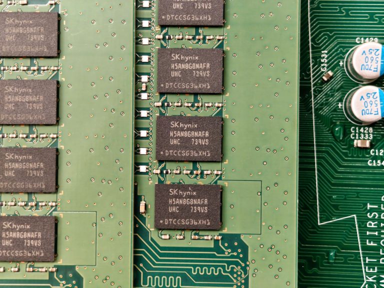
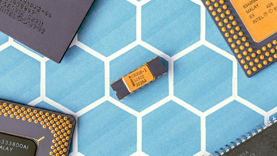
The newly inaugurated facility is not a wafer fab but a high-volume OSAT plant, a crucial link in the semiconductor value chain. While wafer fabrication (front-end) creates the integrated circuits, OSAT (back-end) involves packaging the bare silicon dies, testing them for functionality, and preparing them for integration into end products. For telecom operators and network equipment manufacturers, this stage is vital for producing the System-on-Chip (SoC) units, power management ICs, and RF modules that power 5G base stations, core network routers, customer premises equipment (CPE), and smartphones.
The CG Semi JV, approved by the Indian government in February 2025, involves a total investment of Rs 7,600 crore (approximately $915 million). The facility is projected to have a production capacity of 15 million units per day. While specific process node details for the packaging technology were not disclosed, the involvement of Renesas—a global leader in automotive and industrial semiconductors—and Stars Microelectronics, a specialized OSAT player, suggests capabilities in advanced packaging techniques like Fan-Out Wafer-Level Packaging (FOWLP) and System-in-Package (SiP). These are increasingly important for creating the compact, high-performance, and power-efficient chips required for next-generation telecom infrastructure and devices. The facility’s location in the Gujarat Industrial Development Corporation (GIDC) estate in Sanand positions it within an emerging electronics manufacturing cluster, benefiting from existing infrastructure and a skilled workforce pipeline.
Impact on Telecom Operators and Network Infrastructure Ecosystem

The operationalization of India’s first major OSAT facility under the India Semiconductor Mission (ISM) has direct and profound implications for the telecom sector’s resilience, cost structure, and innovation cycle.
Supply Chain De-risking: The global telecom industry remains acutely vulnerable to geographic concentration in semiconductor manufacturing, with over 90% of advanced chip production and a significant portion of assembly and test located in East Asia. The COVID-19 pandemic and subsequent geopolitical tensions exposed this fragility, leading to extended lead times and price volatility for essential components. For Indian mobile network operators (MNOs) like Reliance Jio, Bharti Airtel, and Vodafone Idea, and for equipment vendors such as Sterlite Technologies, Tejas Networks, and global players with local manufacturing like Nokia and Ericsson, a domestic OSAT capability shortens the supply chain. It reduces dependency on imports for assembled chips, potentially lowering logistics costs and improving inventory management for critical network rollout and maintenance components.
Cost Competitiveness and Local Sourcing: The government’s Production Linked Incentive (PLI) scheme for telecom and networking products mandates increasing levels of domestic value addition. A local OSAT facility enables equipment manufacturers to source packaged semiconductors from within India, helping them meet PLI criteria and qualify for fiscal benefits. This could translate into more competitive pricing for 5G radios, fiber optic terminal equipment, and enterprise networking gear for Indian telcos. Over time, as scale increases, it could make India a cost-competitive manufacturing base for export-oriented telecom hardware production.
Catalyst for Indigenous Design and Innovation: The presence of a reliable, high-volume OSAT partner within the country is a significant enabler for fabless semiconductor design houses. Indian chip design firms, which already contribute significantly to the global talent pool, can now more feasibly design chips specifically tailored for the Indian telecom market—such as for low-cost 4G/5G CPE, ruggedized IoT modules for utilities, or optimized power amplifiers for sub-6 GHz spectrum. They can partner with CG Semi for prototyping and volume production, reducing time-to-market and fostering a homegrown innovation ecosystem around telecom silicon.
Strategic Implications: Positioning India in the Global Telecom Hardware Landscape
The launch of the CG Semi facility is not an isolated event but a cornerstone of India’s broader strategy to become a “semiconductor nation” and a trusted alternative in the global electronics value chain. This has specific ramifications for the telecom infrastructure market in Asia and globally.
Building a “China+1” Hub for Telecom Equipment: Global telecom operators and hyperscalers are actively diversifying their supplier bases away from over-reliance on any single geography. India, with its massive domestic market, engineering talent, and now growing semiconductor ecosystem, is positioning itself as a primary “China+1” destination. The OSAT facility adds a critical layer of vertical integration. For instance, a company could design a 5G small cell chip in Bangalore, have it fabricated at a foundry in Taiwan or South Korea, and then ship the wafers to Sanand for final packaging, testing, and integration into a housing manufactured elsewhere in India. This end-to-end capability within a trusted jurisdiction is a powerful attractor for foreign direct investment in telecom manufacturing.
Synergy with Other Semiconductor Initiatives: The CG Semi OSAT complements other approved semiconductor projects under the ISM, including the Tata Group’s proposed DRAM fab and the Tata-PSMC foundry for legacy logic chips. While these fabs will take years to become operational, the OSAT facility can immediately serve the packaging needs of global fabless companies and integrated device manufacturers (IDMs), building operational expertise and credibility. For the telecom sector, a mature local OSAT industry is a prerequisite for attracting investment in more specialized front-end fabs focused on analog, mixed-signal, and RF processes—the very chips that form the backbone of wireless communication.
Addressing the Legacy Node Gap: Much of the focus in semiconductor discussions is on cutting-edge sub-7nm nodes for CPUs and GPUs. However, the telecom infrastructure world relies heavily on mature nodes (28nm to 65nm and above) for power management, RF transceivers, microcontrollers, and sensors. These nodes are currently in severe global shortage due to underinvestment. India’s strategy, evidenced by partnerships like Tata-PSMC, targets this legacy node space. The CG Semi OSAT is perfectly aligned to package these types of chips, directly addressing a key bottleneck in the production of 5G macro and small cells, fiber optic line terminals, and smart meters.
Forward-Looking Analysis: The Road Ahead for Telecom Semiconductors in India
The inauguration of the Sanand facility is a promising start, but its long-term success and impact on the telecom sector hinge on several factors. First, achieving competitive yield rates and cost structures will be paramount. OSAT is a low-margin, high-volume business; CG Semi must rapidly ramp production and demonstrate world-class quality to attract anchor customers from the telecom equipment and smartphone OEM world. Second, the development of a robust ecosystem of material suppliers, equipment maintenance providers, and specialized engineering talent around the facility is essential to ensure smooth operations and continuous technology upgrades.
For telecom operators, the strategic implication is to begin engaging with this nascent supply chain. Proactive MNOs could partner with domestic equipment makers and CG Semi to co-develop or specify requirements for custom chipsets for network functions, potentially leading to optimized performance for Indian network conditions and spectrum allocations. Regulators, on their part, must ensure policies remain stable and incentives are disbursed efficiently to sustain investor confidence for the long gestation periods inherent in semiconductor projects.
In conclusion, Prime Minister Modi’s launch of the CG Semi OSAT plant is a seminal event for India’s telecom infrastructure ambitions. It moves the country from being a pure consumer of semiconductor technology to becoming an active participant in its production. While challenges remain, this facility lays the groundwork for a more resilient, innovative, and cost-effective telecom hardware ecosystem in India, with ripple effects that will be felt across the global network equipment supply chain for years to come.
About the Author