Source: ETTelecom – In a strategic pivot that will reshape the semiconductor supply chain underpinning global telecom networks, Synopsys Inc. has announced it will discontinue its manufacturing process control software, used by major chip foundries to detect production anomalies. The company will reallocate those resources toward high-margin AI-driven chip design tools. This move, reported on July 7, 2026, signals a profound shift in the electronics design automation (EDA) industry’s priorities, with direct consequences for the production yield, cost, and timeline of the advanced semiconductors powering 5G/6G RAN, core network switches, and edge computing infrastructure.
The End of an Era for Foundry Process Control Software

Synopsys’s decision targets its Yield Explorer and Process Explorer software suites, critical tools for statistical process control (SPC) in semiconductor fabrication plants (fabs). These applications analyze vast datasets from wafer production—measuring parameters like layer thickness, etching depth, and electrical characteristics—to identify yield-limiting defects and process variations in real-time. For years, this software has been integral to maintaining high yields and consistent quality in the manufacturing of complex chips, including application-specific integrated circuits (ASICs) for network processors, RF front-end modules, and optical transceivers.
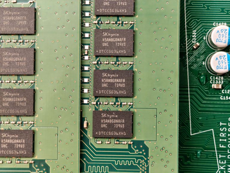
The company informed customers that it will cease development and sales of these manufacturing-oriented products, with a final end-of-life (EOL) support date expected within the next 18-24 months. This exit is a direct result of Synopsys’s internal resource reallocation to capitalize on the booming demand for AI-accelerated EDA tools. The market for AI-powered chip design software is forecast to grow at a compound annual growth rate (CAGR) exceeding 25%, far outpacing the more mature, lower-margin fab control software segment. Major customers like SK Hynix and Samsung have reportedly been notified and are already pivoting to in-house developed solutions, a trend that could accelerate vertical integration and proprietary tool development among leading memory and logic chipmakers.
Telecom Network Hardware Supply Chain at an Inflection Point

For telecom equipment manufacturers (TEMs) and network operators investing in Open RAN, cloud-native core networks, and disaggregated hardware, the Synopsys move introduces new layers of complexity and risk to an already strained supply chain.
Yield Impacts on Cost and Availability: High-performance telecom silicon, such as 5nm and 3nm system-on-chips (SoCs) for massive MIMO radios or 800G/1.6T optical DSPs, requires exceptionally high yields to be economically viable. A reduction in third-party, best-in-class process control software could lead to a short-term dip in yield optimization at fabs, potentially increasing unit costs and constraining supply for critical components. Ericsson, Nokia, Huawei, and newer Open RAN radio unit (O-RU) vendors depend on a steady, cost-effective supply of these advanced chips.
Rise of Proprietary Fab Software: The shift by SK Hynix and Samsung toward in-house solutions highlights a broader industry trend of vertical integration. While this may insulate large, integrated device manufacturers (IDMs) from third-party software dependencies, it raises the barrier to entry for smaller, fabless chip designers serving niche telecom markets. A fabless company designing a novel power amplifier or beamforming IC may find it harder to access the same level of sophisticated process control at a foundry if the standard toolkit is diminished.
Accelerated AI Design for Network Silicon: The capital flowing into AI design tools is not without potential upside for telecom. Synopsys’s DSO.ai and similar platforms from Cadence and Siemens EDA use AI to optimize chip layouts for performance, power, and area (PPA). This could lead to faster design cycles for next-generation network processors optimized for AI-native RAN intelligent controllers (RICs) or energy-efficient chips for cell site routers, potentially accelerating innovation cycles.
Strategic Implications for Global Telecom Infrastructure Development

The reallocation of EDA investment from manufacturing control to AI design reflects a fundamental bet on the future of computing. For the telecom sector, this has distinct regional and strategic ramifications.
U.S. and European Fab Ambitions: Initiatives like the U.S. CHIPS Act and the European Chips Act aim to rebuild domestic semiconductor manufacturing capacity. These new or expanded fabs will require state-of-the-art software stacks. The retreat of a major vendor like Synopsys from the fab control market could create an opening for new software entrants or increase reliance on tools from Applied Materials, KLA, or homegrown solutions. It also places greater emphasis on workforce skills in data analytics and machine learning for fab operations.
Asia-Pacific Supply Chain Dominance: The decision reinforces the strategic autonomy of leading Asian chipmakers. Samsung and SK Hynix’s move to internal tools demonstrates their advanced capabilities and reduces external dependencies. For telecom operators globally, this means the cost and innovation trajectory of memory (crucial for network buffering and caching) and leading-edge logic chips remain tightly controlled by a few vertically integrated giants in South Korea and Taiwan.
Impact on “Chiplet” and Advanced Packaging: A key trend in telecom hardware is the use of chiplets and advanced packaging (e.g., 2.5D, 3D-IC) to combine specialized dies for RF, digital, and photonics. These heterogeneous integration techniques require exquisite process control during assembly and testing. If the software ecosystem for monitoring these back-end processes fragments, it could slow the adoption of these performance-enhancing, cost-reducing technologies in network equipment.
Forward-Look: A More Integrated, AI-Dependent Hardware Ecosystem

Synopsys’s strategic exit from fab control software is a bellwether for the semiconductor industry’s future: design intelligence is being prioritized over manufacturing optimization in the value chain. For the telecom sector, this heralds a period of adaptation.
Network operators and their hardware suppliers must engage more deeply with their semiconductor partners to understand the evolving toolchain landscape and its impact on roadmap reliability. Procurement strategies may need to account for potential volatility in component costs due to yield fluctuations. Conversely, the accelerated development of AI-optimized silicon promises a new generation of network equipment with vastly improved performance-per-watt, a critical metric for sustainable network expansion.
The long-term outcome may be a bifurcated ecosystem: mega-fabs with proprietary, AI-driven manufacturing stacks producing the bulk of advanced components, and a niche market for third-party fab control software serving smaller foundries and research facilities. Telecom’s journey toward software-defined, open, and intelligent networks is, ironically, becoming more dependent than ever on the proprietary, hardware-centric decisions made in the EDA boardrooms of Silicon Valley.
About the Author