
Tata’s 90nm Chip Strategy: A Pragmatic Launch for India’s Telecom Infrastructure Ambitions
📰Original Source: ETTelecomTata Electronics is set to launch India’s first domestically produced semiconductor wafers using a mature 90-nanometer (nm) technology node, according to a report by ETTelecom. This strategic move, supported by the Indian government’s $10 billion semiconductor incentive scheme, marks a critical, albeit pragmatic,…
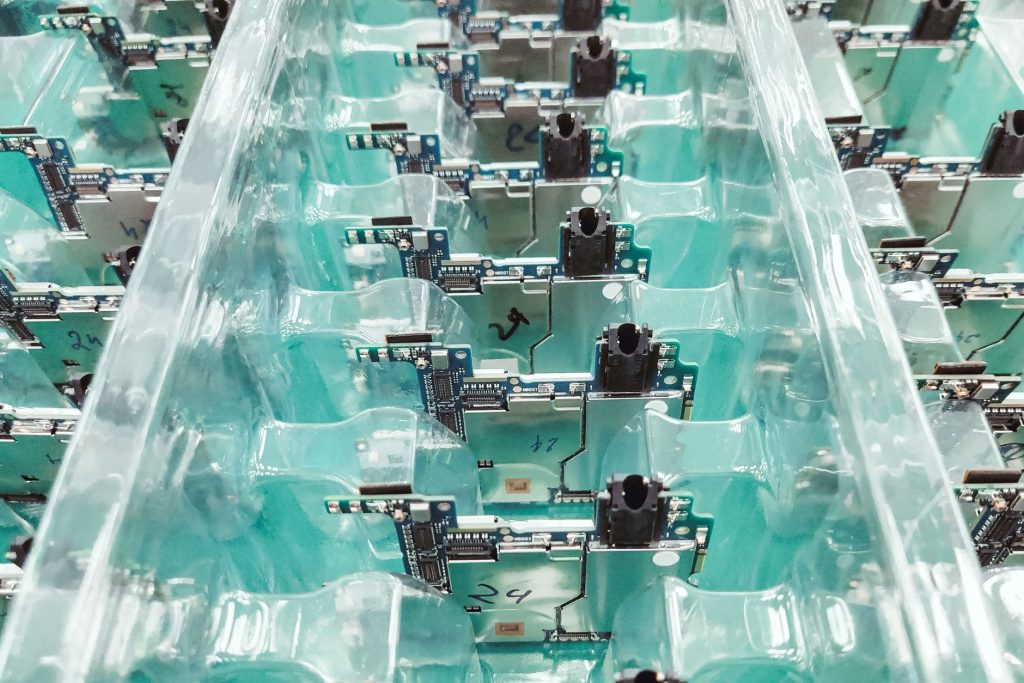
Tata Electronics is set to launch India’s first domestically produced semiconductor wafers using a mature 90-nanometer (nm) technology node, according to a report by ETTelecom. This strategic move, supported by the Indian government’s $10 billion semiconductor incentive scheme, marks a critical, albeit pragmatic, first step in establishing a sovereign chip ecosystem. For the telecom sector, this development signals the beginning of a long-term supply chain diversification strategy, targeting foundational components for network infrastructure, IoT devices, and power management systems, rather than competing directly in the advanced processor race dominated by TSMC and Samsung. The initial production will leverage a legacy 90nm process, with a more advanced 28nm fabrication plant (fab) planned for Dholera, Gujarat, in partnership with Taiwan’s Powerchip Semiconductor Manufacturing Corp. (PSMC).
The Technical and Strategic Rationale for Mature Node Manufacturing

The decision to commence production on a 90nm node, a technology first commercialized in the early 2000s, is a calculated entry point for India’s nascent semiconductor industry. While consumer headlines focus on cutting-edge 3nm and 2nm processes for smartphones and AI chips, a vast segment of the global semiconductor market—and the telecom equipment sector in particular—relies on these mature and legacy nodes. The 90nm to 28nm range is the workhorse for analog, mixed-signal, and power management integrated circuits (PMICs), which are ubiquitous in network hardware.
From a technical and economic standpoint, starting with a mature node offers several advantages. The capital expenditure (CapEx) for a 90nm fab is significantly lower than for a sub-10nm extreme ultraviolet (EUV) lithography facility. The process technology is well-understood, stable, and yields are high, reducing technical risk for a first-time entrant. Furthermore, the equipment is more readily available and not subject to the same export control restrictions as the most advanced lithography tools. This allows Tata Electronics and its partner PSMC to rapidly establish production capacity and begin the critical process of building a skilled domestic workforce—from fab technicians to process engineers.
The real strategic target is the subsequent 28nm facility in Dholera. The 28nm node represents a crucial inflection point, often described as the “last full-node” where performance, power efficiency, and cost are optimally balanced for a wide array of applications. It is the dominant technology for a significant portion of microcontrollers (MCUs), connectivity chips (Wi-Fi, Bluetooth, LTE Cat-1), display drivers, and automotive electronics. For telecom, 28nm is perfectly suited for many baseband processors in IoT modules, network interface cards, and edge computing appliances. By establishing a beachhead at 90nm, Tata is building the operational and supply chain foundation necessary to successfully ramp the more complex and commercially significant 28nm node.
Implications for Telecom Operators and Network Infrastructure

The development of domestic semiconductor manufacturing has profound, long-term implications for telecom network operators (MNOs), tower companies, and equipment vendors. In the short term, the impact is minimal, as global supply chains for components like optical transceivers, routers, and radio units remain dominated by established players like Broadcom, Marvell, Intel, and Qualcomm. However, the strategic intent is clear: to reduce critical dependencies and secure the hardware foundation of India’s digital infrastructure.
For Indian MNOs like Reliance Jio, Bharti Airtel, and Vodafone Idea, a local chip supply chain could eventually translate into greater control over equipment costs, customization for local network conditions, and improved supply chain resilience against geopolitical disruptions. Components such as Power Management ICs (PMICs) for base stations, Ethernet PHY chips for backhaul, and MCUs for smart grid applications in tower power systems are ideal candidates for initial localization. This aligns with the government’s Production Linked Incentive (PLI) schemes for telecom gear, creating a synergistic push for “Made in India” from the chip level upward.
Globally, infrastructure vendors like Nokia, Ericsson, and Huawei may view this as both a competitive threat and a partnership opportunity. As geopolitical pressures encourage regionalization of tech supply chains, having a qualified local fab for certain non-leading-edge components could become a strategic advantage for vendors serving the Indian and broader South Asian markets. We may see joint development agreements or technology licensing deals between Tata Electronics and global telecom chip designers to create India-specific variants of network silicon.
Regional Dynamics and the Broader Asian Semiconductor Landscape

India’s entry into chip manufacturing reshapes the strategic map of semiconductor production in Asia. While Taiwan (TSMC, PSMC), South Korea (Samsung), and China (SMIC) lead in advanced logic, and Singapore and Malaysia specialize in packaging and testing, India is carving out a niche in mature-node manufacturing with massive domestic demand as its anchor. This “India for India” strategy, supported by government capital, is a direct response to supply chain vulnerabilities exposed during the COVID-19 pandemic and ongoing US-China tech tensions.
The partnership with Taiwan’s PSMC is particularly noteworthy. PSMC is a specialist in foundry services for mature and specialty technologies, including power semiconductors and display driver ICs. This collaboration provides Tata with immediate access to proven process technology and operational know-how, bypassing a decade of painful in-house R&D. It mirrors similar strategies seen in other regions, such as the partnership between GlobalFoundries and Abu Dhabi’s Mubadala.
For the broader MENA and African telecom markets, India’s success could provide a model for other regions seeking greater technological sovereignty. While building a full-scale fab requires immense capital and expertise, the focus on mature nodes for critical infrastructure components is a more achievable goal. African nations with ambitions to develop local device assembly or network equipment production could eventually source foundational chips from a regional partner like India, rather than relying solely on East Asian supply chains. This could foster a new axis of South-South cooperation in telecom hardware.
Forward-Look: From Silicon to Systems Integration
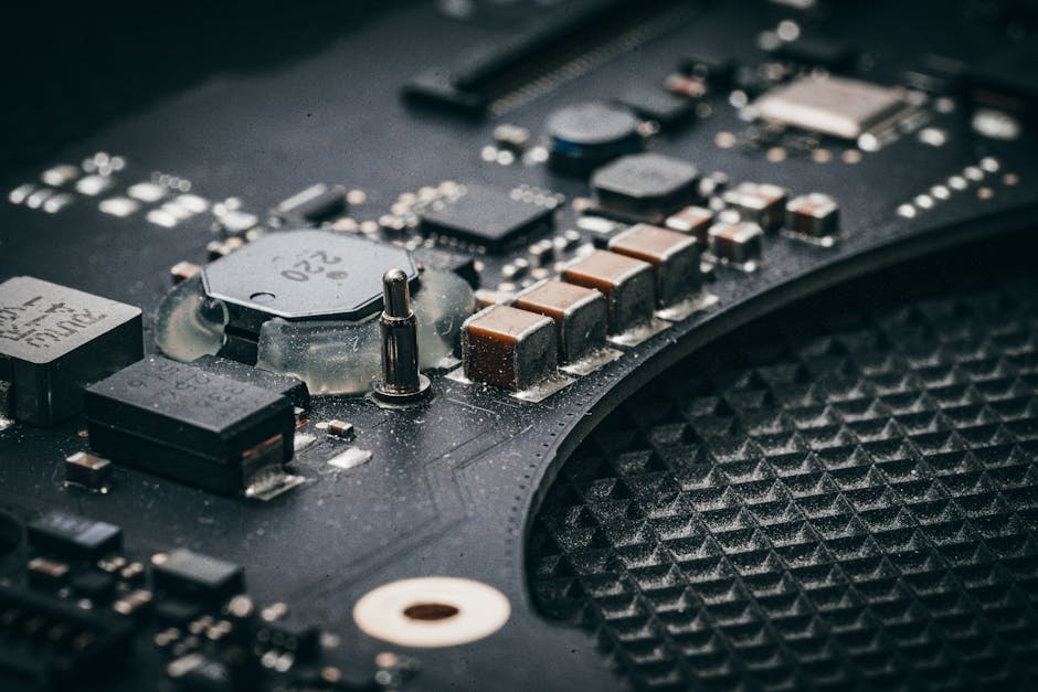
The launch of 90nm wafer production is just the first transistor in a much larger circuit. The true measure of success for Tata Electronics and India’s semiconductor mission will be its integration into viable commercial products and systems. The next 3-5 years will be focused on yield improvement, quality certification, and attracting design houses to port their legacy and mainstream chip designs to the Indian fab. The telecom industry should monitor several key milestones: the groundbreaking and tool installation at the Dholera 28nm fab, announcements of design wins from Indian or global telecom IC companies, and any partnerships with open RAN (O-RAN) chipset developers.
In the long term, a successful domestic semiconductor industry could enable more radical innovation in network architecture. With control over the silicon, operators and vendors could co-design chips optimized for India’s unique spectrum bands, climate conditions, and energy constraints. This could lead to more efficient, cost-effective, and sustainable network infrastructure tailored for high-growth, price-sensitive markets.
While Tata’s use of “older technology” may seem underwhelming to some, for telecom infrastructure professionals, it represents a shrewd and necessary first step. It builds the foundational capabilities—the cleanrooms, the supply chains, the human capital—upon which a more advanced and strategically vital electronics ecosystem can be constructed. The journey of a thousand miles begins with a 90-nanometer step.