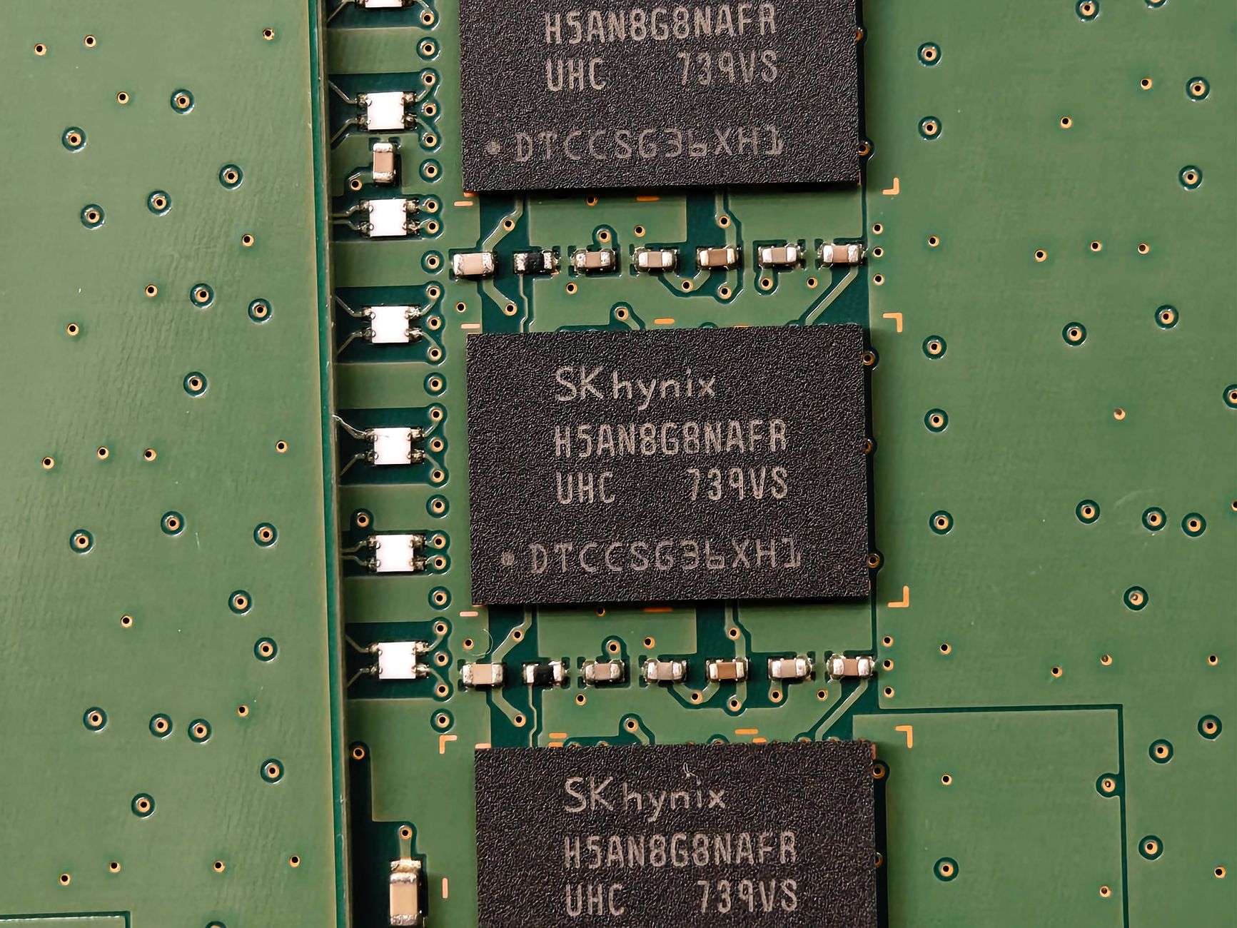
Source: ETTelecom – SK Hynix, the world’s second-largest memory chipmaker and a dominant supplier of High-Bandwidth Memory (HBM) for artificial intelligence accelerators, has announced a strategic plan to begin production of next-generation AI memory chips at a new advanced packaging facility in West Lafayette, Indiana, by the second half of 2029. The move, confirmed by company executives, directly addresses a severe and persistent shortage of HBM chips that the firm forecasts will last through 2030, driven by explosive demand for AI training and inference in data centers. For telecom operators and network infrastructure providers, this long-term supply constraint and the geographic shift in semiconductor manufacturing have profound implications for the availability, cost, and architecture of AI-powered network equipment, from core routers to Open RAN radios and edge compute nodes.
Technical Deep Dive: HBM4E, Advanced Packaging, and the AI Memory Bottleneck

The Indiana facility will focus on the production of High-Bandwidth Memory (HBM), a critical component stacked vertically alongside AI processors like NVIDIA’s GPUs and Google’s TPUs to provide the massive, ultra-fast data throughput required for large language model training. SK Hynix’s roadmap targets the production of HBM4E, the expected fourth generation of the HBM standard, at this site. HBM4 is projected to offer significantly higher bandwidth and capacity than the current HBM3E generation, with data transfer rates potentially exceeding 2 terabytes per second (TB/s) per stack and stack heights increasing to 16-high or more.
The core challenge driving the shortage is not merely wafer fabrication but advanced packaging. HBM production requires intricate processes like Through-Silicon Via (TSV) technology and thermal compression bonding to vertically stack multiple DRAM dies. This packaging capacity is scarce globally. SK Hynix’s $3.87 billion investment in Indiana, supported by U.S. CHIPS Act funding, is specifically for an Advanced Packaging plant. This “fab-lite” strategy complements its wafer fabs in South Korea, decoupling the packaging bottleneck from the front-end semiconductor line. The 2029 timeline underscores the complexity and lead time required to establish this cutting-edge capacity. For telecom equipment manufacturers (TEMs) like Nokia, Ericsson, and Cisco, whose next-generation products increasingly integrate AI-specific silicon (ASICs, DPUs, NPUs), securing a stable supply of co-packaged HBM will be a critical competitive factor, influencing product roadmaps and launch schedules well into the next decade.
Industry Impact: Supply Chain Realignment, Cost Pressures, and Network Equipment Design
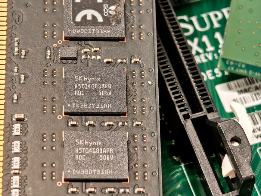
The forecasted memory shortage through 2030 creates a multi-faceted impact on the telecom industry. Firstly, it introduces sustained cost and availability pressures for AI-optimized networking hardware. Cloud service providers (AWS, Azure, Google Cloud), major purchasers of such gear for their hyper-scale data centers, will likely have priority access to HBM supply through strategic partnerships with SK Hynix and its competitors (Samsung, Micron). This could squeeze availability for traditional TEMs and smaller operators, potentially delaying or increasing the cost of network upgrades.
Secondly, the supply chain is undergoing a geopolitical and logistical realignment. The Indiana plant is a direct response to U.S. policy aimed at reducing dependency on Asian semiconductor manufacturing. For U.S.-based telecom operators and federal network projects, this onshoring effort may eventually provide a more secure, albeit potentially more expensive, supply chain for critical infrastructure components. It also aligns with broader trends in “secure by design” network architectures being promoted by governments in North America and Europe.
Finally, the HBM shortage will influence hardware design philosophies. Network equipment designers may be forced to optimize AI workloads for less memory-intensive architectures or explore alternative memory technologies like GDDR6X for certain inference tasks at the edge. The scarcity will accelerate the trend towards disaggregation, where software intelligence is decoupled from proprietary hardware, allowing operators to deploy AI functions on commercial off-the-shelf servers where HBM supply might be more fluid, albeit at a performance trade-off.
Strategic Implications for Global Telecom Markets and Edge AI

The ramifications of the AI memory crunch extend unevenly across global telecom markets. In developed markets like North America and Europe, where operators are aggressively deploying AI for network automation, predictive maintenance, and personalized services, the shortage could act as a brake on innovation tempo. Projects reliant on cutting-edge, HBM-dependent hardware for real-time network optimization may face delays. Conversely, it may spur investment in software-centric AI solutions and legacy infrastructure optimization to extract more value from existing assets.
For emerging markets in Africa, the Middle East, and Southeast Asia, the dynamic is different. While these regions are also pursuing AI and digital transformation, their immediate network investments are often more focused on coverage expansion (4G/5G) and fiber backhaul. The HBM shortage’s primary impact may be indirect, manifesting as higher global prices for imported AI-capable core network equipment or longer lead times for advanced mobile core (5GC) and orchestration platforms. However, it also presents an opportunity. By leapfrogging legacy hardware-centric approaches, these markets could adopt cloud-native, AI-as-a-Service models from the outset, reducing dependency on the constrained hardware supply chain. The success of this approach hinges on robust, low-latency connectivity—placing even greater strategic importance on submarine cable landings, terrestrial fiber, and edge data center investments in these regions.
Forward Look: Navigating the Long-Term Semiconductor Constraint in Telecom
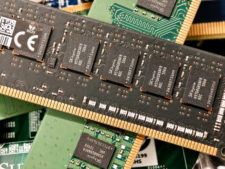
SK Hynix’s Indiana announcement and its 2030 shortage forecast signal a new era for the telecom sector, where access to advanced semiconductors is as strategically vital as spectrum or fiber. Network operators must evolve their procurement and planning strategies. This includes forging deeper, strategic relationships with key suppliers like SK Hynix, engaging in joint technology roadmapping with TEMs, and considering longer-term purchase commitments to secure supply. Infrastructure investment decisions will increasingly need a “silicon availability” risk assessment.
Furthermore, the industry’s push towards Open RAN and virtualized network functions (VNFs) takes on added significance. An open, software-defined architecture provides flexibility to deploy AI workloads across a heterogeneous mix of hardware, potentially mitigating the risk from any single component shortage. The next five years will see a fierce competition not just for AI algorithms, but for the physical silicon that makes them viable at scale within telecom networks. Operators and infrastructure players that successfully navigate this constrained landscape—through strategic partnerships, architectural agility, and diversified sourcing—will gain a decisive advantage in building the intelligent, autonomous networks of the 2030s.
About the Author