
ASML-Tata Electronics Deal for Dholera Fab Marks Strategic Shift in Global Telecom Supply Chain
Source: ETTelecom reports that Tata Electronics has signed a pivotal agreement with Dutch firm ASML to supply advanced lithography tools and solutions for a new semiconductor fabrication plant (fab) in Dholera, Gujarat, marking a foundational milestone in India’s $10 billion semiconductor ecosystem development program.
The strategic partnership, announced during Dutch Prime Minister Rob Jetten’s visit to India, directly addresses a critical vulnerability in the global telecom infrastructure supply chain: the geographical concentration of advanced semiconductor manufacturing. For telecom operators and network equipment providers (NEPs) globally, the establishment of a major fab in India, backed by the world’s sole supplier of extreme ultraviolet (EUV) lithography machines, signals a long-term diversification of sourcing for the chips that power everything from 5G baseband units and optical transport gear to IoT modules and edge computing servers. The Dholera facility, part of Tata’s $11 billion semiconductor investment, is positioned to produce chips on mature 28-nanometer (nm) and older nodes—the workhorse processes for a vast majority of network infrastructure, automotive, and consumer electronics.
Technical Deep Dive: ASML’s Lithography Tools and the 28nm+ Node Imperative
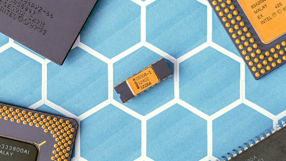
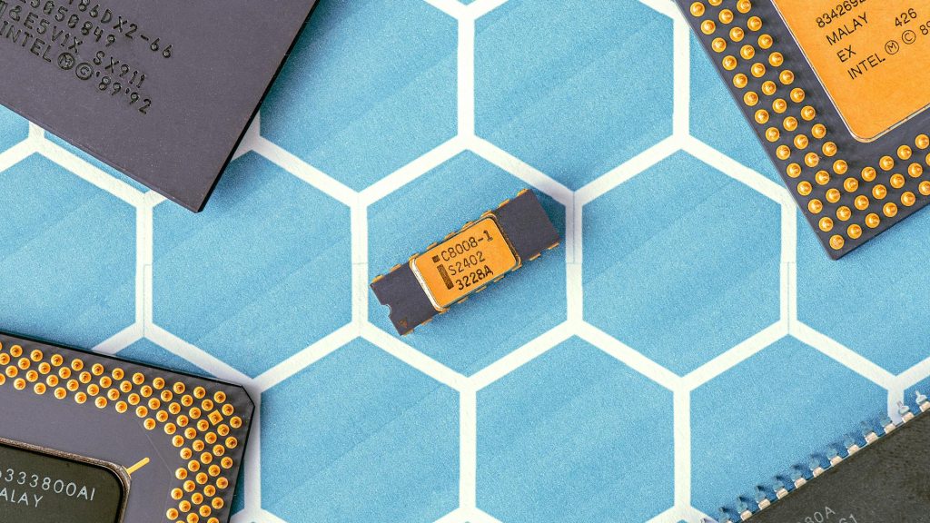
ASML’s agreement with Tata Electronics is not for its cutting-edge EUV systems, which are essential for fabricating sub-7nm chips for high-end smartphones and CPUs, but for its deep ultraviolet (DUV) lithography tools. This is a deliberate and strategically significant choice for the telecom sector. DUV lithography, including ArF immersion and KrF systems, is the proven, high-volume manufacturing technology for nodes from 28nm down to approximately 7nm. The 28nm, 40nm, 55nm, and 65nm nodes represent the “sweet spot” for cost, performance, and power efficiency for a vast array of telecom-specific semiconductors.
These include Power Amplifiers (PAs) and RF front-end modules for 4G/5G base stations, Ethernet PHY chips for switches and routers, optical transceiver drivers, and legacy microcontrollers for network management. The global shortage of these mature-node chips during the COVID-19 pandemic crippled production lines for telecom equipment, causing massive deployment delays for operators. By securing a direct supply line from ASML, Tata’s Dholera fab gains access to the most critical and complex machinery in the semiconductor manufacturing process. Lithography defines the circuit patterns on silicon wafers, and ASML holds a near-monopoly, with over 90% market share in the DUV lithography segment. The deal likely encompasses Twinscan NXT series immersion scanners, which are the industry standard for high-volume 28nm production.
The Dholera Special Investment Region (DSIR) provides the necessary mega-infrastructure: 22,000 acres of land, guaranteed water and power supply, and proximity to a port. The fab’s planned capacity, while not officially disclosed, is expected to be significant, aiming for tens of thousands of wafer starts per month (WSPM). This scale is necessary to impact global supply dynamics. For context, a single 28nm wafer can yield thousands of chips, meaning a single fab can produce hundreds of millions of chips annually, directly feeding into the supply chains of telecom NEPs like Nokia, Ericsson, Cisco, and Huawei, as well as Indian OEMs.
Industry Impact: Reshoring, Diversification, and Cost Dynamics for Telecom Operators

For Mobile Network Operators (MNOs) and telecom infrastructure players, the India-based fab initiative has three primary implications: supply chain resilience, potential cost stabilization, and geopolitical realignment.
First, supply chain diversification moves from boardroom rhetoric to tangible reality. Currently, over 80% of the world’s semiconductor manufacturing capacity, particularly for mature nodes, is concentrated in Taiwan (TSMC, UMC), South Korea (Samsung), and China (SMIC). This concentration creates single points of failure—from geopolitical tensions to natural disasters and pandemics. The establishment of a high-volume, ASML-equipped fab in India creates a credible alternative source. Operators pushing for network densification (5G, fiber deep) and IoT expansion can demand that their equipment vendors diversify their chip sourcing. This reduces the risk of future shortages that could stall network rollouts and service expansions.
Second, while initial production costs in India may not undercut established fabs in East Asia, the long-term cost dynamics could become favorable. The Indian government’s Production Linked Incentive (PLI) scheme for semiconductors provides financial support covering 50% of project costs. Combined with a large domestic talent pool and growing local demand, this could lead to competitive pricing for mature-node wafers over the next 5-7 years. For operators, this could translate into more stable, and potentially lower, equipment prices over the long term, as vendor supply chains become more robust and less prone to inflationary shocks from concentrated production hubs.
Third, the deal has significant geopolitical and regulatory dimensions. The US-led CHIPS Act and its allied partnerships aim to reduce dependency on Asian semiconductor manufacturing. India’s entry as a major player, with Western technology (ASML is a Dutch company with significant US tech restrictions), aligns with this broader strategy. For operators in Europe, Africa, and the Middle East, sourcing equipment with “India-made” chips could become a strategic preference, offering a neutral alternative amidst US-China trade tensions. It also empowers Indian telecom operators like Reliance Jio, Bharti Airtel, and Vodafone Idea with a potential “home-field” advantage in securing supply for their massive network modernization and 5G rollout programs.
Regional Implications: Catalyst for India’s Telecom-Tech Ecosystem and MENA/Africa Connectivity
The Tata-ASML deal is the cornerstone of a larger ambition: to create a vertically integrated electronics and telecom manufacturing ecosystem in India. A domestic source of semiconductors will act as a magnet for downstream industries.
1. Network Equipment & Device Manufacturing: Companies like Dixon, Foxconn, and Salcomp, which already assemble smartphones and other devices in India, will have a powerful incentive to also establish high-value printed circuit board (PCB) assembly and final system integration for telecom gear. The ability to source chips locally reduces import bills, shortens lead times, and allows for more responsive product customization for the Indian market—such as cost-optimized 5G radios for rural coverage or specific IoT modules for agriculture and logistics.
2. “China+1” Strategy for Global NEPs: Global network equipment providers, under pressure from governments and investors to de-risk their supply chains, are actively pursuing a “China+1” manufacturing strategy. India, with its large market, skilled workforce, and now a foundational semiconductor industry, becomes the most logical “+1.” We can expect accelerated investments from Ericsson, Nokia, Samsung Networks, and even Jabil and Sanmina in expanding their Indian manufacturing footprints, moving from simple assembly to more complex subsystem manufacturing.
3. Impact on MENA and African Telecom Markets: For operators in the Middle East, Africa, and South Asia, India’s emergence as a semiconductor and telecom hardware hub offers a geographically and politically proximate sourcing alternative. Shipping times and costs from India to Mombasa or Dubai are significantly lower than from East Asia. This could lead to faster deployment cycles and more affordable network equipment in these high-growth markets. Furthermore, Indian NEPs like Tejas Networks (now part of Tata) and STL could leverage domestic chip supply to develop and export competitively priced, customized optical and wireless solutions for emerging markets, challenging the dominance of traditional Western and Chinese vendors.
Forward-Looking Analysis: The Long Road to Telecom Supply Chain Sovereignty

The Tata-ASML pact is a monumental first step, but the journey to a resilient, diversified semiconductor supply chain for telecom is measured in years, not quarters. The Dholera fab will likely take 3-4 years to become fully operational and ramp to high-volume yield. In the interim, the global telecom industry remains dependent on existing supply chains.
However, the strategic direction is now clear. We anticipate a wave of ancillary investments in India around semiconductor materials, specialty gases, wafer testing, and advanced packaging—all critical parts of the value chain. For telecom CTOs and procurement heads, this development warrants a strategic review of vendor sourcing policies and long-term equipment roadmaps. Engaging with vendors on their India manufacturing and chip sourcing plans will become a key part of contract negotiations.
Ultimately, the success of this venture will depend on consistent policy support, continuous skill development, and the ability to achieve global-scale cost competitiveness. If successful, the Dholera fab will not just be an Indian asset but a global one, fundamentally altering the geopolitical and economic map of the telecom infrastructure industry and providing a much-needed buffer against future disruptions in the silicon supply chain that underpins the entire digital world.